- 您现在的位置:买卖IC网 > Sheet目录463 > IXTN62N50L (IXYS)MOSFET N-CH 500V 62A SOT-227
IXTN62N50L
Symbol Test Conditions
(T J = 25 ° C Unless Otherwise Specified)
Characteristic Values
Min. Typ. Max.
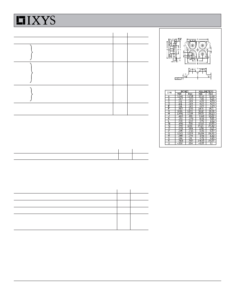
SOT-227B (IXTN) Outline
g fs
V DS = 10V, I D = 0.5 ? I D25 , Note 1
10
15
20
S
C iss
11.5
nF
C oss
C rss
V GS = 0V, V DS = 25V, f = 1MHz
1460
210
pF
pF
t d(on)
t r
t d(off)
t f
Q g(on)
Q gs
Q gd
Resistive Switching Times
V GS = 15V, V DS = 0.5 ? V DSS , I D = 0.5 ? I D25
R G = 2 Ω (External)
V GS = 20V, V DS = 0.5 ? V DSS , I D = 0.5 ? I D25
36
85
110
75
550
115
180
ns
ns
ns
ns
nC
nC
nC
(M4 screws (4x) supplied)
R thJC
0.156 ° C/W
R thCS
Safe Operating Area Specification
0.05
° C/W
Symbol
Test Conditions
Characteristic Values
Min. Typ. Max.
SOA
V DS = 400V, I D = 750mA, T C = 90 ° C
300
W
Source-Drain Diode
Symbol Test Conditions
(T J = 25 ° C, Unless Otherwise Specified)
Characteristic Values
Min. Typ. Max.
I S
I SM
V SD
t rr
V GS = 0V
Repetitive, Pulse Width Limited by T JM
I F = I S , V GS = 0V, Note 1
I F = I S , V GS = 0V
500
62
176
1.5
A
A
V
ns
-di/dt = 100A/ μ s, V R = 100V
Note 1. Pulse test, t ≤ 300 μ s, duty cycle, d ≤ 2%.
IXYS Reserves the Right to Change Limits, Test Conditions, and Dimensions.
IXYS MOSFETs and IGBTs are covered
4,835,592
4,931,844
5,049,961
5,237,481
6,162,665
6,404,065 B1
6,683,344 6,727,585 7,005,734 B2
7,157,338B2
by one or moreof the following U.S. patents: 4,850,072
5,017,508
5,063,307
5,381,025
6,259,123 B1
6,534,343
6,710,405 B2 6,759,692 7,063,975 B2
4,881,106
5,034,796
5,187,117
5,486,715
6,306,728 B1
6,583,505
6,710,463
6,771,478 B2 7,071,537
发布紧急采购,3分钟左右您将得到回复。
相关PDF资料
IXTN90N25L2
MOSFET N-CH 90A 250V SOT-227
IXTP02N50D
MOSFET N-CH 500V 200MA TO-220
IXTP05N100M
MOSFET N-CH 1000V 700MA TO-220
IXTP08N120P
MOSFET N-CH 1200V 800MA TO-220
IXTP100N04T2
MOSFET N-CH 40V 100A TO-220
IXTP10N60PM
MOSFET N-CH 600V 5A TO-220
IXTP12N50PM
MOSFET N-CH 500V 6A TO-220
IXTP130N065T2
MOSFET N-CH 65V 130A TO-220
相关代理商/技术参数
IXTN79N20
功能描述:MOSFET 79 Amps 200V RoHS:否 制造商:STMicroelectronics 晶体管极性:N-Channel 汲极/源极击穿电压:650 V 闸/源击穿电压:25 V 漏极连续电流:130 A 电阻汲极/源极 RDS(导通):0.014 Ohms 配置:Single 最大工作温度: 安装风格:Through Hole 封装 / 箱体:Max247 封装:Tube
IXTN8N150L
功能描述:MOSFET 8 Amps 1500V RoHS:否 制造商:STMicroelectronics 晶体管极性:N-Channel 汲极/源极击穿电压:650 V 闸/源击穿电压:25 V 漏极连续电流:130 A 电阻汲极/源极 RDS(导通):0.014 Ohms 配置:Single 最大工作温度: 安装风格:Through Hole 封装 / 箱体:Max247 封装:Tube
IXTN90N25L2
功能描述:MOSFET 90 Amps 250V RoHS:否 制造商:STMicroelectronics 晶体管极性:N-Channel 汲极/源极击穿电压:650 V 闸/源击穿电压:25 V 漏极连续电流:130 A 电阻汲极/源极 RDS(导通):0.014 Ohms 配置:Single 最大工作温度: 安装风格:Through Hole 封装 / 箱体:Max247 封装:Tube
IXTN90P20P
功能描述:分立半导体模块 -90.0 Amps -200V 0.044 Rds RoHS:否 制造商:Infineon Technologies 产品:Thyristor Power Modules 类型:Phase Controls 安装风格:Screw 封装 / 箱体:DT61 封装:
IXTP 3N100P
制造商:IXYS 功能描述:Bulk
IXTP01N100
制造商:IXYS 制造商全称:IXYS Corporation 功能描述:High Voltage MOSFET
IXTP01N100D
功能描述:MOSFET 0.1 Amps 1000V 110 Rds RoHS:否 制造商:STMicroelectronics 晶体管极性:N-Channel 汲极/源极击穿电压:650 V 闸/源击穿电压:25 V 漏极连续电流:130 A 电阻汲极/源极 RDS(导通):0.014 Ohms 配置:Single 最大工作温度: 安装风格:Through Hole 封装 / 箱体:Max247 封装:Tube
IXTP02N120P
功能描述:MOSFET 500V to 1200V Polar Power MOSFET RoHS:否 制造商:STMicroelectronics 晶体管极性:N-Channel 汲极/源极击穿电压:650 V 闸/源击穿电压:25 V 漏极连续电流:130 A 电阻汲极/源极 RDS(导通):0.014 Ohms 配置:Single 最大工作温度: 安装风格:Through Hole 封装 / 箱体:Max247 封装:Tube
